| Home |
| 01/10/84 BIOS | 06/10/85 BIOS | 11/15/85 BIOS | Comment | |
|---|---|---|---|---|
| 01 | 80286 register test | 80286 register test | 80286 register test | |
| 02 | Verify shutdown byte in 146818 RTC chip | Verify checksum of BIOS ROMs | Verify checksum of BIOS ROMs | For 01/10/84 BIOS, see note 6 |
| 03 | Verify checksum of BIOS ROMs | Verify shutdown byte in 146818 RTC chip | Verify shutdown byte in 146818 RTC chip | |
| 04 | 8254 PIT channel 1 - 'all bits on' test | 8254 PIT channel 1 - 'all bits on' test | 8254 PIT channel 1 - 'all bits on' test | Channel 1 of the 8254 timer chip's 3 channels (0/1/2) |
| 05 | 8254 PIT channel 1 - 'all bits off' test | 8254 PIT channel 1 - 'all bits off' test | 8254 PIT channel 1 - 'all bits off' test | |
| 06 | 8237 DMA #1 - initialization and test | 8237 DMA #1 - initialization and test | 8237 DMA #1 - initialization and test | The first of the two DMA chips (the one in socket U111) |
| 07 | 1. 8237 DMA #2 - initialization and test 2. 8254 PIT channel 1 - initialization |
1. 8237 DMA #2 - initialization and test 2. 8254 PIT channel 1 - initialization |
1. 8237 DMA #2 - initialization and test 2. 8254 PIT channel 1 - initialization |
See note 7 for info on channel 1 initialization |
| 08 | DMA page register test | DMA page register test | DMA page register test | |
| 09 | Memory refresh test | Memory refresh test | Memory refresh test | Verify that dynamic RAM refresh is happening |
| 0A | 8042/8742 - Soft reset | 8042/8742 - Soft reset | 8042/8742 - Soft reset | Issue a soft reset to the motherboard's keyboard controller |
| 0B | 8042/8742 - Self test | 8042/8742 - Self test | 8042/8742 - Self test | Get the motherboard's keyboard controller to do a self test |
| 0C | " " " " " " | " " " " " " | " " " " " " | |
| 0D | 8042/8742 - additional tests | 8042/8742 - additional tests | 8042/8742 - additional tests | |
| 0E | If a warm boot, zero first 64K of base memory | If a warm boot, zero first 64K of base memory | If a warm boot, zero first 64K of base memory | No verification done |
| 0F/DD | Test first 64K of base memory | Test first 64K of base memory | Test first 64K of base memory | On failure, continuously output the POST code of DD (see here) |
| 10 | ||||
| 11 | Speed test | Speed test | See note 1 | |
| 12 | 1. 80286 - additional tests 2. Initialise 8259 PIC #1 |
1. 80286 - additional tests 2. Initialise 8259 PIC #1 |
1. 80286 - additional tests 2. Initialise 8259 PIC #1 |
|
| 13 | Initialise 8259 PIC #2 | Initialise 8259 PIC #2 | Initialise 8259 PIC #2 | |
| 14 | Set up temporary interrupt vectors | Set up temporary interrupt vectors | Set up temporary interrupt vectors | |
| 15 | Set BIOS call interrupt vectors | Set BIOS call interrupt vectors | Set BIOS call interrupt vectors | |
| 16 / 17 | 1. 146818 RTC chip - ask if battery is low 2. 146818 RTC chip - verify checksum |
1. 146818 RTC chip - ask if battery is low 2. 146818 RTC chip - verify checksum |
1. 146818 RTC chip - ask if battery is low 2. 146818 RTC chip - verify checksum |
* POST code 17 is only output if battery is low * Checksum of RAM bytes 14d to 45d within 146818 |
| 18 | Disable parity checking of RAM | Disable parity checking of RAM | Disable parity checking of RAM | Preparation for later |
| 19 | Put 80286 into protected mode | Put 80286 into protected mode | Put 80286 into protected mode | |
| 1A | Verify that 80286 in protected mode | Verify that 80286 in protected mode | Verify that 80286 in protected mode | |
| 1B | Determine size of base memory | Determine size of base memory | Determine size of base memory | See note 2 |
| 1C | Set/reset the 512/640K RAM flag | Set/reset the 512/640K RAM flag | Set/reset the 512/640K RAM flag | |
| 1D | Determine size of extended memory | Determine size of extended memory | Determine size of extended memory | See note 3 |
| 1E | Store extended memory size | Store extended memory size | Store extended memory size | See note 4 |
| 1F | Test address lines 19 to 23 | Test address lines 19 to 23 | Test address lines 19 to 23 | |
| 20 | Exit from protected mode | Exit from protected mode | Exit from protected mode | |
| 21 | Initialise any MDA/CGA video card | Initialise any MDA/CGA video card | Initialise any MDA/CGA video card | |
| 22 | MDA/CGA - Video line test | MDA/CGA - Video line test | MDA/CGA - Video line test | |
| 23 | Process any 'advanced' video card | Process any 'advanced' video card | Process any 'advanced' video card | See note 5 |
| ... | ... | ... | ... | |
| ... | ... | ... | ... | |
| ... | ... | ... | ... |
| DD | See 'OF/DD' above | See 'OF/DD' above | See 'OF/DD' above |
|---|
| Note 1 | Verify that motherboard 'speed' is within certain bounds. Added by IBM to stop the overclocking (via crystal) that owners commonly did to early 5170's. On failure, before halting the CPU, the POST also beeps the speaker: 1 long beep followed by 1 short beep |
| Note 2 | Sizing only. First 64K of base memory was tested at checkpoint 0F. Remainder of base memory gets tested at checkpoint 2F. |
| Note 3 | Executed in protected mode. Sizing only. Extended memory gets tested at checkpoint 2F. |
| Note 4 | Stored in the MC146818 RTC chip |
| Note 5 | Video cards that contain a BIOS ROM. The EGA card is an example. The ROM is executed (i.e. card initialises itself). |
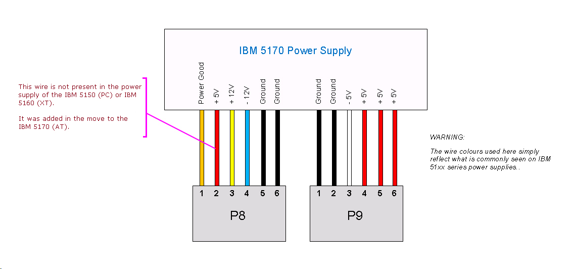
| Note 6 | Failure of the 'Verify shutdown byte' test often occurs when BOTH of the following are true: * Motherboard has the 01/10/84 BIOS * Motherboard inadvertently powered using an XT-class power supply, rather an an AT-class one. |
| Note 7 | Initialise channel #1 of 8254 timer chip, setting a divisor of 18. That results in one output pulse per approx. 15 µs. See here. |